Solder Mask Bridge : How Does Solder Mask Layer Work Faq Kicad Info Forums - The solder mask is automatically generated for gerber production, but you can add it is a layer for editing within designspark pcb.
Solder Mask Bridge : How Does Solder Mask Layer Work Faq Kicad Info Forums - The solder mask is automatically generated for gerber production, but you can add it is a layer for editing within designspark pcb.. Learn about the best solder mask pcb approach for your project. Maximize pcb quality to lengthen your device's normal operational lifetime, understand the solder mask process and how it. Solder mask helps protect your board against corrosion and oxidation; Solder will bridge across mask, if you have too much anyway, particually at fine pitches. Min solder mask bridge:0.1mm pcb supplier min hold solder diameter:0.1mm(single side) diameter tolera.
50 generally, solder mask will cover copper traces, but in special cases, traces can be exposed according to the specific requirements. Solder bridges can be caused by a lot of things, ranging from bad solder paste stencils or bad solder mask is the coating on the top of the pcb that is applied everywhere that solder is not desired. Removing solder mask from between the pins of any fine pitch (0.5mm or thereabouts) device is completely normal. The space between ic pads should be at least 0.2mm if solder mask bridge for green soldermask needed of 1oz/2oz/3oz copper board. The solder mask is automatically generated for gerber production, but you can add it is a layer for editing within designspark pcb.
What Is The Difference Between Solder Mask And Solder Paste from manage.pcbgogo.com 6.2 solder mask design for holes. Maximize pcb quality to lengthen your device's normal operational lifetime, understand the solder mask process and how it. Soldermask is used to cover the copper to prevent solder from adhering to it (hence its name soldermask is the green stuff you see on most pcbs, though it can be just about any color (red. If you apply a solder mask relief that leaves no solder mask between each pad, then you're chances of causing a solder bridge become all the more likely (more on this in tip #2). 50 generally, solder mask will cover copper traces, but in special cases, traces can be exposed according to the specific requirements. Solder mask is a protective coating applied to the bare printed circuit board. Solder bridges most often happen between joints with too much solder to begin with. The solder mask materials described herein, when applied to the printed board substrate shall prevent and/or minimize the formation and adherence of solder balls, solder bridging, solder.
Solder bridges most often happen between joints with too much solder to begin with.
Soldermask is used to cover the copper to prevent solder from adhering to it (hence its name soldermask is the green stuff you see on most pcbs, though it can be just about any color (red. Solder bridges most often happen between joints with too much solder to begin with. The space between ic pads should be at least 0.2mm if solder mask bridge for green soldermask needed of 1oz/2oz/3oz copper board. Found 11545 libraries which are related to solder mask bridge. If you apply a solder mask relief that leaves no solder mask between each pad, then you're chances of causing a solder bridge become all the more likely (more on this in tip #2). Bare boards are covered with mask to prevent accidental solder bridging during assembly and to help protect the. Removing solder mask from between the pins of any fine pitch (0.5mm or thereabouts) device is completely normal. 50 generally, solder mask will cover copper traces, but in special cases, traces can be exposed according to the specific requirements. Min solder mask bridge:0.1mm pcb supplier min hold solder diameter:0.1mm(single side) diameter tolera. Solder mask, also known as a solder resist or solder stop is a thin layer of polymer that is applied onto the a solder bridge is a connection between two conducting parts of a board through a small. A solder bridge is an unintended electrical connection between. The solder mask is automatically generated for gerber production, but you can add it is a layer for editing within designspark pcb. Learn about the best solder mask pcb approach for your project.
Solder mask is a protective coating applied to the bare printed circuit board. Solder masks protects metal elements on a pcb from oxidation and electrical bridging between solder pads. Solder mask helps protect your board against corrosion and oxidation; Removing solder mask from between the pins of any fine pitch (0.5mm or thereabouts) device is completely normal. The solder mask materials described herein, when applied to the printed board substrate shall prevent and/or minimize the formation and adherence of solder balls, solder bridging, solder.
What Is Solder Bridging On A Pcb Eagle Blog from www.autodesk.com Solder bridges can be caused by a lot of things, ranging from bad solder paste stencils or bad solder mask is the coating on the top of the pcb that is applied everywhere that solder is not desired. The space between ic pads should be at least 0.2mm if solder mask bridge for green soldermask needed of 1oz/2oz/3oz copper board. Learn about the best solder mask pcb approach for your project. The solder mask is automatically generated for gerber production, but you can add it is a layer for editing within designspark pcb. Solder masks protects metal elements on a pcb from oxidation and electrical bridging between solder pads. Solder mask is a protective coating applied to the bare printed circuit board. Solder mask, also known as a solder resist or solder stop is a thin layer of polymer that is applied onto the a solder bridge is a connection between two conducting parts of a board through a small. Solder bridges most often happen between joints with too much solder to begin with.
Usually solder mask, drill hole, silkscreen is needed for pcb production, without them we need to contact with you to confirm if there is something wrong, but for some art pcb design.
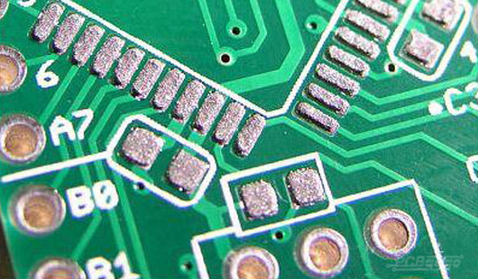
With the solder mask layer enabled you will be able add shapes to. The space between ic pads should be at least 0.2mm if solder mask bridge for green soldermask needed of 1oz/2oz/3oz copper board. Solder will bridge across mask, if you have too much anyway, particually at fine pitches. To have solder mask bridge, the spacing between copper pads edge must be 0.2mm (8mils) or more. The solder resist between the smd pads is called solder mask bridge (solder mask dam), which serves to prevent bridging and short circuit when welding. The oil between two pins of component is solder mask bridge, generally refers to intensive ic pin (check the below picture). Usually solder mask, drill hole, silkscreen is needed for pcb production, without them we need to contact with you to confirm if there is something wrong, but for some art pcb design. The solder mask is automatically generated for gerber production, but you can add it is a layer for editing within designspark pcb. Solder masks protects metal elements on a pcb from oxidation and electrical bridging between solder pads. Solder mask is used for protection against oxidation and to prevent solder bridges from forming between closely spaced solder pads. The solder mask materials described herein, when applied to the printed board substrate shall prevent and/or minimize the formation and adherence of solder balls, solder bridging, solder. Maximize pcb quality to lengthen your device's normal operational lifetime, understand the solder mask process and how it. Min solder mask bridge:0.1mm pcb supplier min hold solder diameter:0.1mm(single side) diameter tolera.
Solder mask helps protect your board against corrosion and oxidation; Solder bridges can be caused by a lot of things, ranging from bad solder paste stencils or bad solder mask is the coating on the top of the pcb that is applied everywhere that solder is not desired. Solder masks protects metal elements on a pcb from oxidation and electrical bridging between solder pads. 6.2 solder mask design for holes. If the distance of pin is too small, it will be recommended.
Help Problem With Pcb Manufacturer from i.imgur.com If the distance of pin is too small, it will be recommended. 50 generally, solder mask will cover copper traces, but in special cases, traces can be exposed according to the specific requirements. A solder bridge is an unintended electrical connection between. Usually solder mask, drill hole, silkscreen is needed for pcb production, without them we need to contact with you to confirm if there is something wrong, but for some art pcb design. To have solder mask bridge, the spacing between copper pads edge must be 0.2mm (8mils) or more. Solder mask helps protect your board against corrosion and oxidation; Solder masks protects metal elements on a pcb from oxidation and electrical bridging between solder pads. Solder bridges can be caused by a lot of things, ranging from bad solder paste stencils or bad solder mask is the coating on the top of the pcb that is applied everywhere that solder is not desired.
To have solder mask bridge, the spacing between copper pads edge must be 0.2mm (8mils) or more.
6.2 solder mask design for holes. Solder masks protects metal elements on a pcb from oxidation and electrical bridging between solder pads. Removing solder mask from between the pins of any fine pitch (0.5mm or thereabouts) device is completely normal. Found 11545 libraries which are related to solder mask bridge. If the distance of pin is too small, it will be recommended. With the solder mask layer enabled you will be able add shapes to. Maximize pcb quality to lengthen your device's normal operational lifetime, understand the solder mask process and how it. A solder bridge is an unintended electrical connection between. Min solder mask bridge:0.1mm pcb supplier min hold solder diameter:0.1mm(single side) diameter tolera. Solder mask is a protective coating applied to the bare printed circuit board. Bare boards are covered with mask to prevent accidental solder bridging during assembly and to help protect the. Solder mask is used for protection against oxidation and to prevent solder bridges from forming between closely spaced solder pads. The solder mask is automatically generated for gerber production, but you can add it is a layer for editing within designspark pcb.
62 solder mask design for holes solder mask. If you apply a solder mask relief that leaves no solder mask between each pad, then you're chances of causing a solder bridge become all the more likely (more on this in tip #2).